Technical report from the lowRISC Summer Internship 2016
Friday, 2nd September, 2016
Xuan Guo, Nathanael Davison, Profir-Petru Partachi, Alistair Fisher
Contents
- Introduction
- License
- Overview of the Project
- Approaching the task
4.1 Codec Discussion
4.2 Specific Objectives
4.3 Previous Work
4.3.1 lowRISC
4.3.2 MPEG-2 Codec - First Steps: Outputting to VGA
5.1 Implementing VGA Specification
5.2 Video Controller
5.2.1 Control Registers
5.2.2 Driver
5.3 Iterations of Video Driver - MPEG-2 Decode Implementation
6.1 Profiling - Infrastructure for Accelerators
7.1 Concept
7.2 Architecture
7.3 Scatter-Gather
7.4 Accelerator Instruction
7.5 Driver
7.5.1 Bare-metal Driver
7.5.2 Linux Driver - Accelerators
8.1 DCT/IDCT
8.1.1 The 1D Row/Column units
8.1.2 The pipeline for 2D DCT/IDCT
8.1.3 The stream processor wrapper for DCT/IDCT
8.2 IDCT Stream processor
8.3 Y’UV 422 to 444
8.4 Y’UV444 to RGB888
8.5 RGB888 to RGB565 - Continuous Integration
9.1 Travis and Linting
9.2 Synthesis and Scripts - Final Results and Evaluation
10.1 Comparison to Project Objectives
10.2 Comparison of Video with and without Acceleration
10.3 Limitations and Design Decisions
10.3.1 Stream Processing
10.3.2 Machine Instructions
10.3.3 Interrupts - Future work
11.1 Memory
11.2 Driver Scatter-Gather Support
11.3 Y’UV 420 to 422 and Interpolation
11.4 General Accelerators
1. Introduction
Beginning on Monday, 27th June 2016, a team of 4 undergraduate students from the University of Cambridge joined the lowRISC project for a 10 week internship, kindly sponsored by IMC Financial Markets. The purpose of this report is to provide a technical description of the work undertaken and the devices produced. This will allow others to understand and continue with the work in the future, or to contribute to the lowRISC chip in a similar fashion. For information on how to use the accelerators and infrastructure produced during the internship, without the technical description, please see the appropriate tutorial. All development was done using the Digilent Nexys 4 DDR board, which uses a Xilinx Artix-7 FPGA. All source code can be found on github.
2. License
3. Overview of the Project
The objective of our internship was to take the current lowRISC System-on-Chip design and demonstrate how an interested individual or team could extend it and add an accelerator of their own. After some initial discussion, we decided to aim to extend the current lowRISC SoC design to enable video output, with the final goal of playing video smoothly at a resolution of 640x480 on our Nexys 4 DDR FPGAs.
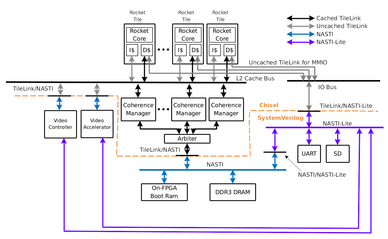
This task was decomposed into several milestones: adding VGA functionality to lowRISC, adding an in-memory framebuffer, implementing a video codec for RISC-V, and designing and creating 2D accelerators to allow real-time video decoding, with the majority of the work being in the development of the accelerators. The planned architecture for the augmented SoC is shown in the the diagram below, with the new elements being the Video Accelerator and the Video controller. Communication is performed over the AXI protocol. The implementation of AXI we used was called NASTI (‘Not A STandard Interface’) by its authors. All future references to AXI use the NASTI name.
In order to fully satisfy the goal of demonstrating how others might use the lowRISC SoC, in addition to developing our accelerators it was necessary to produce full documentation so our work could be reproduced. To achieve this, we decided we would produce a number of tutorials explaining how to use the infrastructure and devices we created, and a technical report (this document) describing the details of the devices produced.
4. Approaching the Task
4.1 Codec Discussion
We quickly decided we’d follow an existing video codec standard and either implement it ourselves or fork an existing free implementation. A myriad of possibilities are available due to the wide range of existing video formats. The limitations of the FPGAs we were working with narrowed the selection considerably as options such as H.265 were just too computationally taxing to work with. We ended up with a shortlist of three: VP8 (WebM), MPEG-2 (H.262) and MPEG-4 AVC (H.264). Ultimately, we decided on MPEG-2 because of a readily available reference implementation (under a BSD-like license) and its relatively low computational complexity compared to the other options.
4.2 Specific Objectives
These were the formal objectives we defined, against which we could evaluate the progress and success of the project:
- Extending lowRISC to decode MPEG-2 encoded video at a resolution of 640x480, and playing at a rate of 8 frames-per-second on our FPGAs*
- Tutorials describing
- Using the video output controller
- Extending lowRISC with new devices
- Adding additional accelerators using our infrastructure
- Technical descriptions of
- The accelerator infrastructure
- The DCT/IDCT hardware device, including the control logic
- The chroma conversion accelerators
*The platform these technical objectives were to be achieved on is the Digilent Nexys 4 DDR board, running the lowRISC chip design. The board provides 63,400 LUTs, 4,860 Kbits of block RAM, and 128 MiB DDR2. The existing lowRISC chip architecture consumes 50,859 logic cells, and provides a 64-bit RISC-V core running at 25MHz.
4.3 Previous Work
4.3.1 lowRISC
Started in early 2015, lowRISC is a not-for-profit organisation working closely with the University of Cambridge and the open-source community. lowRISC is creating a fully open-source, Linux-capable, RISC-V-based System on Chip with the goal of producing a low-cost development board - supporting the open-source hardware community. Other goals are to explore and promote novel security features, to make it simple for companies to make derivative designs, and to create a benchmark design to aid academic research.
4.3.2 MPEG-2 codec
The MPEG-2 codec was defined to resolve the shortcomings on the MPEG-1 codec, and was standardised in 2000. As such many implementations have been produced. Our starting point for getting video running on lowRISC was the reference implementation distributed at mpeg.org (note: part way through the internship the mpeg.org website went down. An archive of the page can be found here). Over the course of the internship we found that this implementation provided a number of features which we did not need and only served to reduce overall performance. We also found that it had not been written with performance in mind, and was not easy to optimise. However by this point our work was tightly coupled with the library, and so it was not feasible to switch to a different implementation. On reflection it would have been wise to schedule more time for software rewriting, or to start from a more modern reference.
5. Outputting to VGA
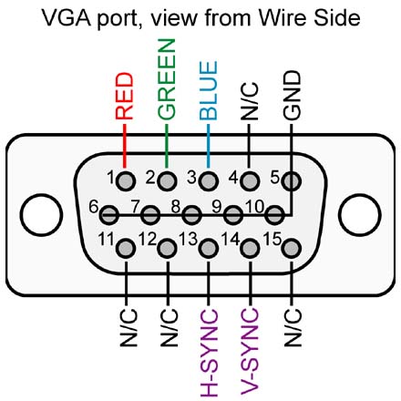
5.1 Implementing VGA Specification
VGA output is controlled by a pair of signals, HSync (horizontal
synchronisation) and VSync (vertical synchronisation) . The timing of these
two signals is used by the monitor to calculate the clock frequency of each
transmitted pixel. The video controller we developed generates R, G, B,
HSync and VSync signals which can be connected to a digital-to-analog
converter (DAC) for VGA output. The colour channels support 8-bit colour per
channel, meaning 24-bit true colour is supported. However, since the DAC on
the Nexys4 DDR board we used is 4-bit only, we are simply ignoring half of the
output pins. A diagram of the VGA ports used is shown here.
5.2 Video Controller
The video controller acts as an I/O slave device by mapping control registers to I/O space; it also acts as a DMA master device fetching frames repeatedly from memory. Currently the video controller is running at a rate of 125MHz, meaning a maximum of 960p video output is supported.
5.2.1 Control Registers
The video controller exposes an AXI-lite interface for communication with the rocket core. The address space of memory mapped control registers is 4096 Bytes, and each register is 32-bits. Therefore we have access to 1024 possible registers. Currently only 18 of them are used.
5.2.2 Driver
To interact with the video driver in bare metal, you need to manipulate the above registers by yourself. A helper header video.h is provided with macro defined.
In Linux, a driver is provided to register the video controller as a framebuffer, so you can use standard framebuffer operation to deal with this device.
6. MPEG-2 Decode Implementation
As mentioned in section 4.3, we used the MPEG-2 implementation distributed on mpeg.org as the starting point for decoding video on the lowRISC chip. The reference implementation provided functionality for outputting each frame to a number of formats, including Y’UV frames, SIF, PPM, and others. With this we then began modifying the library to allow outputting to the frame-buffer described in the previous section, rather than a file. Since the frame-buffer required raw RGB values, the basis of our function was the PPM output function.
6.1 Profiling
To identify useful opportunities for acceleration, we performed profiling of the reference implementation using GNU gprof, a performance analysis tool for Unix applications. The data was gathered on an Intel i5 processor, and so while not being exactly representative of how the codec would run on the FPGA-based lowRISC configuration we’re targeting, it allowed us an insight into the high-level function calls of the program.
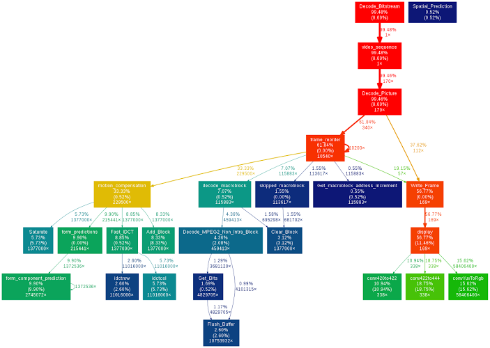
This diagram represents the call graph of the program, and is colour coded according to the percentage of time spent within each function. A number of candidates for acceleration can be identified, such as form predictions, IDCT operations, and chroma conversions. The chroma conversions, labelled on the diagram as conv420to422, conv422to444, and convYuvToRgb, especially present an excellent candidate for acceleration since they are well-defined operations which are guaranteed to be at the end of a video compression pipeline
We also performed some cache analysis using Cachegrind, part of the Valgrind tool suite. Again, this was run on x86 machines, so it only provided an approximation of performance on lowRISC. The results gave some context to the output from the profiling, for example telling us that the display branch of the above tree does most of the memory I/O in the program and that conv422to444 has a poor cache hit rate which explains why it takes longer than the surrounding calls.
7. Infrastructure for Accelerators
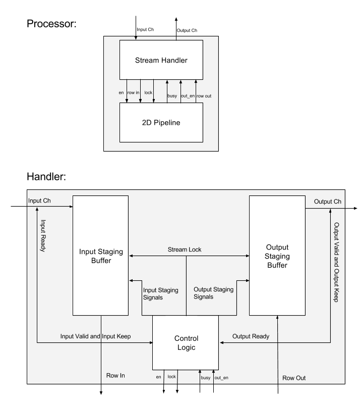
In this section, we will cover the infrastructure of our General Purpose Stream Pipelined Accelerator (SPA).
7.1 Concept
Over the course of development the design has evolved. We started with a much more specialised video accelerator, but have ultimately arrived at a more purpose accelerator infrastructure supporting all kinds of AXI4-Stream compatible processors.
The fundamental idea behind this accelerator idea is streams. In our case, most data can be processed independently, so can be abstracted as separate streams streams. For streams, we can make use of pipelining the reduce number of clock cycles needed to process data. All accelerators in this infrastructure have a pair of AXI4-Stream interface as their only I/O. Data is piped into the accelerator by AXI4-Stream slave port on the accelerator, and piped out from AXI4-Stream master port. Our infrastructure has no direct communication with the accelerators, but uses packet concept in AXI4-Stream as the boundary between data. The infrastructure is only responsible for packet routing and data moving.
7.2 Architecture
This is the third iteration of the architecture design.
Originally we were planning to use DMA to move data into local BRAM, and then processing on BRAM. This design was quickly abandoned due to poor extensibility. It also introduced lots of duplicate control logic but they are so tightly coupled that we could not modularize it easily.
The idea of stream came into play at this stage, inspired by Java’s Stream IO. Most data to be accelerated has good locality, meaning that it does not depend on data further away. In this case, it is natural to abstract them into continuous byte packets. There is still a control unit in this iteration, responsible for receiving instructions, interpret them, and send them to data movers.
In the current architecture, the control unit is removed, and we are sending
commands to data movers directly. The data mover will set T_DEST
accordingly, and the crossbar will be responsible for data forwarding. By
adapting this design, stream processors can be piped to another, as long as
T_DEST is correctly set. We also benefit from standardized interface by
embracing AXI4-Stream specification.
7.3 Scatter-Gather
During development, we’ve found that we need scatter-gather support to speed things up. Due to existence of the MMU, we can only guarantee physical address continuity within the page, which obviously limits the use case of our accelerator. We address this issue by adding scatter-gather support to the data movers, and use a last bit in the every data move command to identify if this command is the last one in the packet.
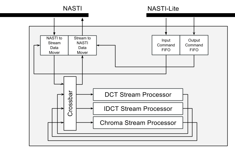
7.4 Accelerator Instruction
The accelerator has two FIFOs: input command FIFO and output command FIFO. The first one controls the data mover moving data into the accelerator and the other one controls the opposite direction. Routing will take place automatically by internal crossbar.
| 63-56 | 55 | 54-40 | 39 | 38-6 | 5-3 | 2-0 |
|---|---|---|---|---|---|---|
| Attributes | Last | Length | Reserved | Address | Reserved | Opcode |
The length field is 15-bit long, this contains 6th to 20th bit of the actual length, with lower 6-bits padded with 0. Address field is the same, it contains 6th to 38th bit of actual length with lower 6-bit padded with 0. This design supports 39-bit physical address, which is the same as what lowRISC current supports.
Data movers in both direction use the same format, however attributes, last, and opcode fields are ignored by data moving which moves data back to the memory.
The last field is the critical field for scatter-gather support: A stream is terminated if last is set to high.
7.5 Driver
Currently two drivers are provided, one for bare metal and one for Linux.
7.5.1 Bare-metal Driver
This is a very basic driver provided without scatter-gather support. In bare metal without MMU enabled, blocks are physically contiguous so scatter-gather is not supported.
Three functions are provided in bare-metal:
// Issue an command to execute an stream processor
void videox_exec(int func, void* src, void* dest, size_t size, int attrib);
// Wait for all issued command to finish
void videox_wait();
// Do memory copy using the accelerator
void* fast_memcpy(void* dest, void* src, size_t size);
7.5.2 Linux Driver
The driver registers a miscellaneous device. The device file only support one operation, which is ioctl. Within a driver, a queue is maintained internally, and the external exposed interface mimics the one in bare metal.
// Query if all issued command are finished
int ret;
ioctl(fd, 0, &ret);
// ret will be 1 if some instructions are still in FIFO

// Issue an instruction to video accelerator
struct request {
    void* src;
    void* dest;
    size_t len;
    int opcode;
    int attr;
};
struct request req = {...};
ioctl(fd, 1, &req);
// Note req.src, req.dest, req.len must be 64-byte aligned
There are few limitations in the current driver. Memory mapping and memory allocation happens in each frame so the accelerator is not useful is amount of data is tiny. Lack of interrupt also cause us to rely on polling to determine whether the command is finished.
8. Accelerators
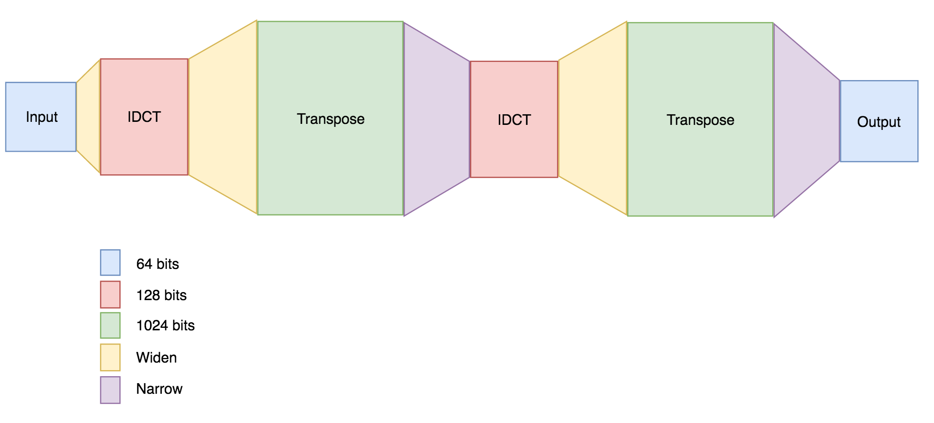
In the final design, 3 special purpose accelerators were written for optimising tasks on the MPEG-2 decode process. These accelerators were for performing the Inverse-Discrete-Cosine-Transform (and the related Discrete-Cosine-Transform), Y’UV 422 to Y’UV 444 upsampling, and the conversion of Y’UV 444 to RGB. Technical descriptions of these can be found in the following section.
8.1 DCT/IDCT
Similar to how we can represent numbers using digits, we can also represent functions with an equivalent of digits, basis functions. One particular way of performing this task is using complex exponentials. If we take only the real part of these basis functions we obtain what is called a cosine transform. Of particular interest to us is the discrete version of this transform due to some of its mathematical properties.
DCT and IDCT are used in video compression to make the data more susceptible to entropy coding by reducing the number of terms required to express the data. This is possible due to the energy compacting nature of DCT. Using knowledge about how we perceive images and zeroing terms that are of little perceptual impact, it is possible to reproduce, after a DCT -> Quantization -> Inverse Quantization -> IDCT phase, an image that is very much similar to the original.
DCT is performed when encoding data, and when using a differential coder or motion compensation, IDCT is used in encoding as well. This is why DCT is usually left unoptimized as it is seen as an offline task.
IDCT is performed during decoding and hence must be able to run on lower end machines than DCT and be performed online/real-time. In our implementation, we have chosen to move IDCT(and as a pair DCT) into hardware as there is sufficient literature with regards to this task as well as the familiarity with these operations from our courses. Our design is as follows:
8.1.1 The 1D Row/Column units
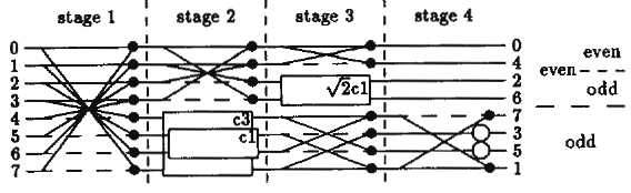
Figure 1: The computation network for DCT-2 [1].
Here, $kC_n$ represents a rotation by $\frac{n*\pi}{16}$ multiplied by the scalar $k$, dotted lines represent negation, dark dots represent addition and non-filled bubbles represent multiplication by a scalar (here $\sqrt2$).
The IDCT computation network is the same as DCT but executed in reverse order, i.e. from right to left.
The 1D units can be used both on rows and columns without modification. No floating point operations are necessary as dyadic fractions (fractions of the form $\frac{n}{2^\alpha}$) are used to approximate the irrationals involved in the rotation and scaling operations. Do, however, note that fixed point multiplication is in fact used in both 1D units.
Input:
| Variable | Description |
|---|---|
row |
Packed array of size 8 of integers* |
en |
Boolean used to signal valid input |
lock |
Boolean used to freeze the internal state |
Output:
| Variable | Description |
|---|---|
idct_row/dct_row |
Packed array of size 8 of integers** |
out_en |
Boolean used to signal valid output |
*The size of the integers is determined by COEF_WIDTH (default: 32)
** The output size is COEF_WIDTH + 2 to reduce errors due premature
truncation
Things to note:
out_enis used in the 2D pipeline to activate the next stage. Whenout_enis low, the output is a zero vector.- The
locksignal is used to freeze the state of the unit in scenarios where we may wish to stall.
8.1.2 The pipeline for 2D DCT/IDCT
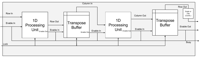
The 2D unit is formed of two 1D units and two transpose buffers connecting them. The pipeline has to be fully flushed between $8\times8$ blocks that are within a single burst to avoid cross-pollution between them.
Input:
| Variable | Description |
|---|---|
row |
Packed array of size 8 of integers* |
en |
Boolean used to signal valid input |
lock |
Boolean used to freeze the internal state |
Output:
| Variable | Description |
|---|---|
idct_row/dct_row |
Packed array of size 8 of integers** |
busy |
Boolean used to signal that there is still in-flight data |
out_en |
Boolean used to signal valid output |
* The size of the integers is determined by COEF_WIDTH (default: 32)
** The output size is COEF_WIDTH + 4 to reduce errors due premature
truncation
Things to note:
- The first result is ready $24$ cycles after the first input for DCT, $26$ for IDCT.
- Intermediary results are provided one per cycle after the first one.
- The last result is ready $16$ cycles after the last input for DCT, $18$ for IDCT.
- If you input a non-multiple of $8$ rows, the missing ones are zero rows and may cause unexpected results. The output is always a multiple of $8$ number of rows.
- Each 1D unit increases the width of the integers by $2$ and as such the output is of size
COEF_WIDTH + 4, and truncation happens as the last stage (combinational logic) post Scale/Clip. - Before inputting to the pipeline check the
busysignal as it is held high from the first input until the pipeline has been cleared of all in flight data. - The
locksignal is used to freeze the state of the unit in scenarios where we may wish to stall.
8.1.3 The stream processor wrapper for DCT/IDCT
The wrapper sets the integer size to $16$ (COEF_WIDTH = 16) and assumes a
64-bit data width bus. Working from this assumption, we can load one row to
the pipeline from the data stream in $2$ cycles. Similarly for output, we can
send the data of a row via the stream in $2$ cycles. The choice was made as a
trade-off between requiring fewer cycles to load/store the data and having a
big enough range of numbers to cover the target use scenarios.
8.2 IDCT Stream processor
A second iteration of the IDCT processor was a pure stream processor that was made possible with the addition of the AXI-stream widener and narrower. In this version we create a multi-stage stream processor that takes in a stream that was widened to provide one full row of data per tick. We then widen the stream again to provide the full matrix ($8 \times 8$ block) in one tick to the transpose unit for the sake of simplifying transpose logic, which is then narrowed to provide one row per tick to the second IDCT unit. Finally, we pass it through a second transpose unit so that the results provided are identical to the software implementation. This flow can be more easily seen diagrammatically as such:
Input/Output:
| Variable | Description |
|---|---|
in_ch |
The input AXI-stream channel |
out_ch |
The output AXI-stream channel |
The stream handler uses the lock signal to stall the pipeline as necessary
for routine load/store or when either input or output is not ready.
A stream_lock signal is used for the situation when either input or output
is not ready so that the handler maintains the current state until we no
longer need to stall. This signal is generated via combinational logic from
the state of in_ch and out_ch.
The output is a stream of at least the same length as the input, however, since it is a stream, we do not concern ourselves with the length as its end will be denoted by a last signal.
Do note that incomplete inputs cause unexpected numeric results by padding zero rows required so that the output is guaranteed to form an integer number of $8\times8$ blocks.
8.3 Y’UV 422 to 444
Chroma sub-sampling is a common compression technique in image encoding which implements less resolution for colour (UV) than for brightness (Y’) information. In Y’UV422 the colour values are sampled at half the rate of the brightness. In order to convert to RGB, we need to reintroduce this resolution somehow. The accelerator we developed does this by simply repeating every colour value twice. A more advanced system would be to interpolate the value of the colour from the surrounding pixels, however this is left as an extension.
The input to the processor is the standard Y’UV422 packed format, shown below.
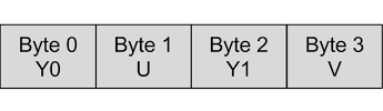
The output is the standard Y’UV444 packed format, shown below. A zero byte is padded on the end in order to bring the packet up to 32 bits, and allows the possibility of future extensions using alpha-values.
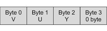
The stream processor infrastructure uses a packet size of 64 bits, and so on each cycle we read in 2 sets of Y’UV422 values. Since we output 2 Y’UV444 values for each Y’UV422 value, we must output at twice the rate we input. In order to do this the device is implemented as an implicit state machine.
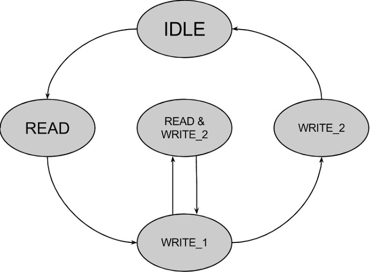
When the src.t_valid signal is set by the data source, we enter the READ
state, record the Y’UV422 data from the src.t_data wire into a buffer, and
set the src.t_ready signal to low in order to prevent more data being sent
before it can be processed. We then enter the WRITE_1 state. In this state
we output the first 2 packets of Y’UV444 data on the dst.t_data wire and
assert dst.t_valid. We then remain in this state until the destination has
asserted dst.t_ready, and so the data transfer has occurred. We then
transition to the READ & WRITE_2 state in which we wait until we can write
the second 2 packets of Y’UV444 data on the dst.t_data wire and assert
dst.t_valid. Once dst.t_ready is also asserted, we assert src.t_ready
for a cycle, read the next packet, and transition back to WRITE_1. We
alternate between these states until the data transfer is complete, at which
point we write the final data packet, assert dst.t_last, and enter the
IDLE state.
While this state machine was the basis of the design, optimisation on the source led to the definition of the state machine being somewhat obfuscated in the code, and appearing as a number of independent states. The transitions are controlled by set of ‘guards’ which only allow the data to move to the next stage of the pipeline if the correct conditions are met.
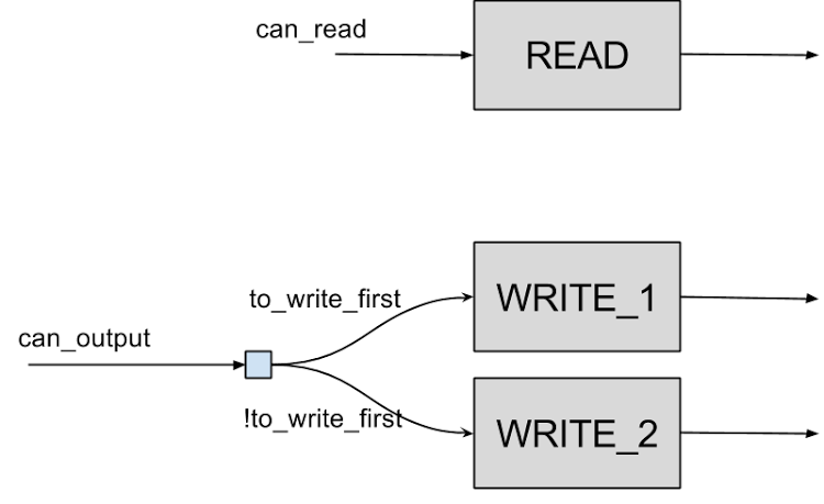
These guards are linked in such a way to allow the correct operation of the state machine.
8.4 Y’UV444 to RGB888
The final stage of decoding is to convert each pixel value from Y’UV to RGB values, the standard for most monitors. The conversions between these is defined as follows:
$C = Y’ - 16$ $D = U - 128$ $E = V - 128$
$R = clamp((298 \times C + 409 \times E + 128) >> 8)$
$G = clamp((298 \times C - 100 \times D + 208 \times E + 128) >> 8)$
$B = clamp((298 \times C + 516 \times D + 128) >> 8)$
where $clamp()$ denotes clamping a value to the range of $0$ to $255$.
Since this operation involves a number of large multiplications and additions this operation is pipelined in order to stay within the timing constraints. The pipeline is shown below.
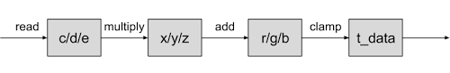
In the first stage, once src.t_valid is set by the source, we read the data
and perform the initial subtractions to generate the $C$, $D$, and $E$ values.
In the multiply stage, we perform all the intermediate multiplications for
calculation $R$, $G$, and $B$. These multiplications are as follows:
$x_0 = 298 * c$
$y_0 = 100 * d$
$y_1 = 516 * d$
$z_0 = 409 * e$
$z_1 = 208 * e$
These multiplications are independent and so occur in parallel. The next stage
is the add stage, which computes the final RGB values by combining the
$x$,$y$,$z$ values of the previous stage. Finally we perform the clamping and
outputting to dst.t_data in one stage.
8.5 RGB888 to RGB565
In order to reduce the memory requirement of frames, RGB values were encoded as 16-bit rather than 24-bit RGB. This was necessary due to the limited resources of the FPGA. We used the standard 16-bit encoding of RGB values - that is 5 bits for red and blue, and 6 bits for green.
The coding of this module is very simple due to the use of a
nasti_stream_widener. The widener handles the fact that for every 64 bits
input we only output 32-bits by buffering the first 32 bits until the next 32
bits are ready. Therefore the converter simply pipes the protocol values to
the narrower, manipulating the RGB values to use the correct bits. The
manipulation is as follows:
assign widener_ch.t_data  = {src.t_data[55:51],  // R
                             src.t_data[47:42],  // G
                             src.t_data[39:35],  // B

                             src.t_data[23:19],  // R
                             src.t_data[15:10],  // G
                             src.t_data[ 7: 3]}; // B
8.6 Saturation and Mismatch Control
In MPEG-2, before feeding data into IDCT, clamping take place first to limit the value from -2048 to 2047. A parity correction took place as well to make sure that sum of all data words is even.
The pseudo code works like this:
static void Saturate(Block_Ptr)
short *Block_Ptr;
{
  int i, sum, val;

  sum = 0;

  /* ISO/IEC 13818-2 section 7.4.3: Saturation */
  for (i=0; i<64; i++)
  {
    val = Block_Ptr[i];

    if (val>2047)
      val = 2047;
    else if (val<-2048)
      val = -2048;

    Block_Ptr[i] = val;
    sum+= val;
  }

  /* ISO/IEC 13818-2 section 7.4.4: Mismatch control */
  if ((sum&1)==0)
    Block_Ptr[63]^= 1;

}
9. Continuous Integration
Continuous integration is a development practice that requires programmers to integrate their code into a shared repository several times a day, with the goal of reducing merge conflicts and catching bugs early. For this to be effective, an automated build and test process is required. lowRISC already had an automated test process using the cloud based Travis CI continuous integration service and Docker. We extended this with a linting step, and set up some independent FPGA based tests.
9.1 Travis and Linting
Linting is the process of analysing source code to flag potential issues. During the build process, Verilator lints the input Verilog files and displays warnings. Unfortunately, many of these are spurious, so we’ve written a short script that attempts to refine them (identifying important warnings using regular expressions). This script is run during the automated testing, if there are any remaining warnings after it has run, the build is considered a failure.
9.2 Synthesis and Scripts
Travis CI is cloud based, which has many benefits, but a significant downside is that HDL code can only be tested via simulation. We found that several errors only manifest when running on the FPGA, so it was desirable to automate some FPGA tests to run alongside Travis.
We did this by having a local machine (with an FPGA turned on and plugged in) periodically poll our main Github repository, when it discovered a new commit, it pulled it and ran some FPGA tests using the new code. It reported the result back to Github once it was finished, typically about half an hour later.
10. Final Results
10.1 Comparison to Project Objectives
A number of project objectives were described in section 4.2. In this section we will discuss each objective and whether it was met, and what could have been improved.
- Decoding MPEG-2 encoded video at a resolution of 640x480, and playing at a rate of 8 frames-per-second
This objective was not met. Once integrated into lowRISC and synthesised on our Naxys4 DDR FPGAs, our accelerators allowed us to decode 320x480 video at a rate of approximately 2.5 frames-per-second. The limiting factor on decoding proved to be the speed we were able to access memory through the TileLink bus. This problem was further compounded by the fact that a bug forced us to disable the L2 cache, and we were unable to resolve it before the end of the project. The speed of the bus had been reduced to 25MHz due to the floating point unit, and so more effort could have been expended on removing the FPU, and increasing the speed of the bus.
- Tutorials describing
- Using the video output controller
- Extending lowRISC with new devices
- Adding additional accelerators using our infrastructure
These tutorials have been completed, and can be found on the lowRISC website.
- Technical descriptions of
- The accelerator infrastructure
- The DCT/IDCT hardware device, including the control logic
- The chroma conversion accelerators
These technical descriptions are included in this document.
10.2 Comparison of Video with and without Acceleration
In order to compare the performance with and without acceleration, we introduced instrumentation into the codec before and after the functions for interacting with the accelerator. In this way we were able to capture the time taken to perform these functions with and without the accelerators. The data was gathered over a video of 658 frames and the values presented an average over all frames in the video.
| Function | Software | Hardware | Speed-up |
|---|---|---|---|
| Y’UV 422 to 444 | 726ms | 20.9ms | 34.7 |
| Y’UV 444 to RGB | 216ms | 26.7ms | 8.08 |
| RGB 32 to 16 | 59.7ms | 10.4ms | 5.71 |
| Total for Frame | 448ms | 160ms | 2.80 |
Table: Time taken to perform accelerated tasks with and without accelerator
It is clear to see that for each of the individual accelerators provide a significant reduction in the CPU time needed for processing, with the conversion of Y’UV 444 to RGB gaining a speed-up of over 8 times. However due Amdahl’s law, the overall speed-up of the full process proved to be significantly less.
One significant factor which reduced the performance of the accelerated codec was the need for a number of memory accesses between each accelerator. The accelerators used memory as the communication medium for passing data. Performing this for each accelerator in each frame lead to a significant limiting of the performance obtained. In order to resolve this we introduced hardware pipe-lining, which allowed accelerators to be chained and data passed directly from one to the next. The effect of hardware pipelining can be seen below.
| Mode | Time | Speed-up (over software) |
|---|---|---|
| Software | 448ms | - |
| Hardware (Unpipelined) | 160ms | 2.80 |
| Hardware (Pipelined) | 103ms | 4.33 |
Table: Time taken to perform frame processing with and without hardware pipelining
As can be seen, hardware pipelining provided a significant speed-up over the unpipelined version. This further illustrates that, with our accelerators, the bottleneck to decoding is the speed memory can be accessed.
10.3 Limitations and Design Decisions
10.3.1 Stream Processing
Stream processing was a useful paradigm for acceleration of IDCT and simple interpolation, since it is very easy to simply stream the video data and have the processors work on it as it flows through. However the lack memory locations and lengths made it very difficult to perform certain tasks such as interpolation and converting Y’UV 420 to Y’UV 422 without a significant amount of buffering.
10.3.2 Machine Instructions
An early discussion during the project was how best to accelerate the codec, by extending RISC-V with support for SIMD instructions, or by adding a memory mapped instruction buffer, placing our defined instructions into the buffer, and having the accelerator driver poll the size of the buffer for instructions in flight.
Of these options, extending the instructions set with SIMD instructions was the most elegant and appealing options. However it was a little beyond the scope of our project, since we lacked the expertise and time to do it properly. We had a discussion about the possibility of using RoCC, but decided to stick with a memory mapped accelerator for the simpleness and ability to support internally.
10.3.3 Interrupts
As mentioned in an earlier section, the accelerator driver we implemented has no support for interrupts, and relies on polling for detecting when instructions are present or complete. As such the driver is less responsive than would be the ideal. In addition it is polling from user-space, which means each poll initialises a system call, taken a considerable number of cycles to complete.
11. Future work
11.1 Memory
During development a deadlock condition arose when interacting with the L2 cache. The exact cause of the deadlock proved to be difficult to reproduce quickly, and so did not arise in simulation at all. The cause seemed to be some interaction between cached and uncached transactions on the TileLink bus. This may be a bug in Rocket’s TileLink implementation, but we were unable to fully confirm. Due to the limited time of our internship, and our lack of knowledge of the Chisel language we avoided this problem by removing the L2 cache entirely. As one might expect, this significantly impacted the performance of the codec. Part way through the internship an update to the TileLink github repository made reference to a fix for a ‘L2 Writeback deadlock issue’. Therefore a future development would be to further evaluate this patch to determine if this reflects the issue we encountered, and look to integrate these updates into the lowRISC repository. If not, more work must be done to further isolate the issue.
11.2 Driver Scatter-Gather Support
Currently the linux driver has support for scatter-gather instructions in physical memory, which is contiguous within user-space. A future extension would be to introduce full scatter-gather support - that is including the case where information is not contiguous within user space.
11.3 Y’UV 420 to 422 and Interpolation
The infrastructure we developed used the AXI-Stream bus protocol. This made it very easy to accelerate our streams of data, such as the data for a frame. However the operation of converting Y’UV 420 to 422 requires the duplication of lines in order to reinsert the relevant values. Therefore it is necessary to buffer each line, and then replay it before moving on to the next line. AXI-Stream has no concept of length, and so introduces a challenge of detecting when a line of data has been received, and when it must be replayed.
We come across a similar problem when introducing interpolation for upsampling. Currently when converting from Y’UV422 to Y’UV444 we simply replay the U and V values. It would instead be better to interpolate these values as an average of the values above, below, before and after. This however would require the buffering of 3 entire rows of data, and so presents the same problems as the simple Y’UV 420 to Y’UV 422 transformation required.
An example interpolation using a vertical 1:2 interpolation filter is presented here in C. This formula is for transforming the planar format, and so would need to be manipulated in order to work on the packed format.
yuv444[w * (j-2)] = clamp(( 3 * yuv422[w * (j-3)]
                        -  16 * yuv422[w * (j-2)]
                        +  67 * yuv422[w * (j-1)]
                        + 227 * yuv422[w * j]
                        -  32 * yuv422[w * (j+1)]
                        +   7 * yuv422[w * (j+2)]
                        + 128) >> 8);

yuv444[w * ((2 * j) + 1)] = clamp(( 3 * yuv422[w * (j-3)]
                                -  16 * yuv422[w * (j-2)]
                                +  67 * yuv422[w * (j-1)]
                                + 227 * yuv422[w * j]
                                -  32 * yuv422[w * (j+1)]
                                +   7 * yuv422[w * (j+2)]
                                + 128) >> 8);
11.4 Other Accelerators
The infrastructure we have created is usable for the acceleration of many other tasks. Any task which is amenable to stream processing can be accelerated in this architecture, for example deflate compression, Huffman coding, or context-adaptive variable-length coding (used in MPEG-4). The method for adding an accelerator of this kind is described in the tutorial describing adding an accelerator to the video accelerator.
11.5 Increased CPU Speed
Currently, lowRISC needs to be run at a clock rate of 25 MHz or less due to the FPU. We intentionally designed our system to avoid using any floating point operations, with the intention of removing the FPU and boosting the clock rate to increase performance. Unfortunately, this proved to be too difficult to do in our brief internship, while we successfully removed the FPU and ran the codec, we could not increase the clock rate successfully. This is because the clock rate is tightly coupled with several other components and we didn’t have the time or expertise to adjust everything correctly. A future goal is boosting performance by removing the FPU and doubling the clock rate to 50 MHz.
References
[1] Loeffler C., Lightenberg A., Moschytz G. S., Practical fast 1–D DCT algorithms with 11 Multiplications, Proceedings of the International Conference on Acoustics, Speech and Signal Processing (ICASSP’89), 1989. – P. 988–991.