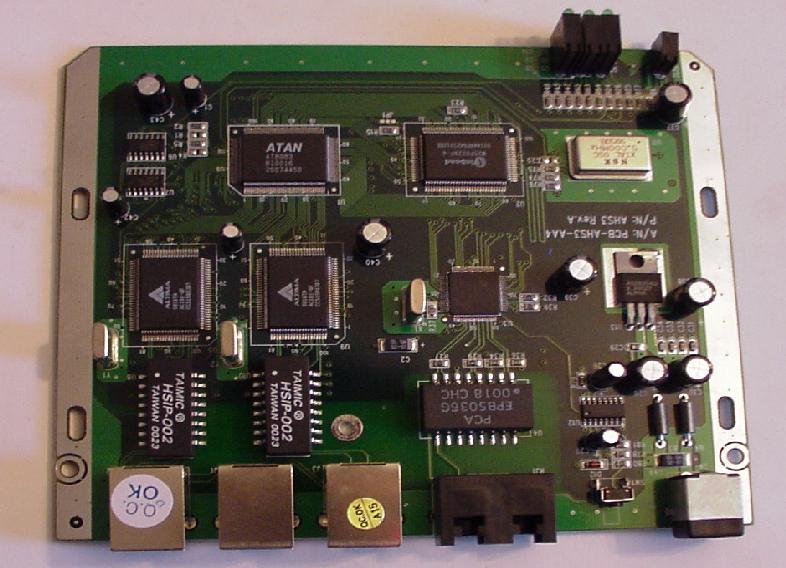
Here is the PCB that is inside the Linksys HPNA 1.0 Hub. This is a three port ethernet switch with one port being HPNA 1.0.
The card has a pair of switched 10baseT ports on the left using three RJ45 connectors. One of the ports is present with both pinout directions, hence three connectors for two ports.
The two RJ11 connectors in the middle are in parallel and connect only the outer two pins. These are the homePNA port and connect to the AMD AM79C901AVC phy device via the magnetics block. There are three differential sets of pads between the PHY device and its magentics, which I guess are TX, RX and CD.
On the right is DC 5 volt input and a reset switch. Top right is a power on LED and a further set of 9 leds for TX, RX and CD on each of the three ports.
Apart from the AMD PHY chip, there are two Altima ethernet port devices and an ATAN AT8993. The Windbond chip is perhaps the SRAM for the packet buffers and bridging tables. Threre are three 74HC chips for the reset and led drive. There are four crystals.